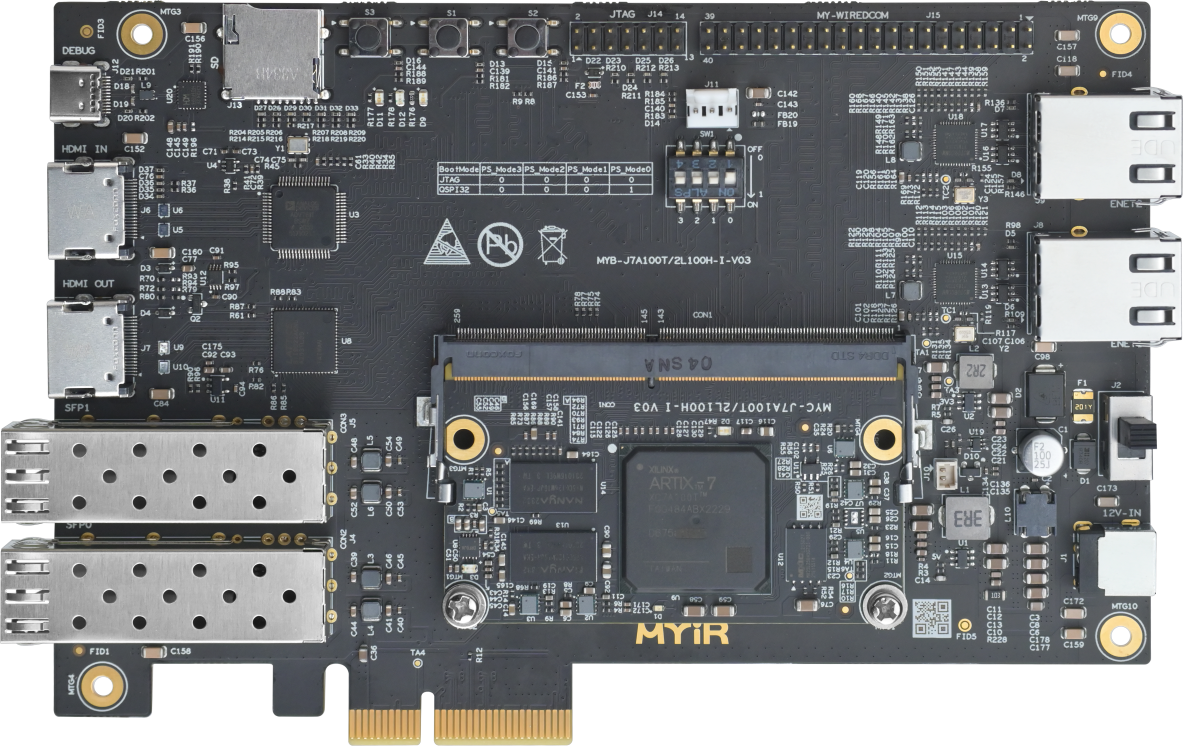
MYIR MYD-J7A100T Development Board Based on AMD/Xilinx XC7A100T Processor
The MYD-J7A100T Development Board comprises the MYC-J7A100T System-On-Module (SOM) and a specially designed base board, which provides a fully equipped platform for evaluating and developing solutions based on AMD/Xilinx Artix-7 FPGAs. The MYD-J7A100T incorporates the XC7A100T (XC7A100T-2FGG484I) device from the Artix-7 series and extends a rich set of peripherals and interfaces on the base board through connectors and headers. These include two Gigabit Ethernet ports, two SFP+ interfaces, a PCIe 2.0 interface, HDMI input and output interfaces, a DVP camera interface, a Micro SD slot, a USB-UART interface, a FAN interface, and a 2.5mm pitch 2x 20-pin IO expansion interface.
Mechanical Parameters
- Dimensions: 167.64mm x 130.65mm (baseboard), 69.6mm x 40mm (SOM)
- PCB Layers: 6-layer design (baseboard), 12-layer design (SOM)
- Power supply: 12V/2A (baseboard), 5V/3A (SOM)
- Working temperature: -40~85 Celsius
The MYC-J7A100T System-On-Module
FPGA
- AMD/Xilinx XC7A100T Artix-7 FPGA (XC7A100T-2FGG484I)
Memory and Storage
- 512MB DDR3
- 32MB QSPI FLASH
- 32KB EEPROM
Signals Routed to Expansion Interface
- 0.5mm pitch 260-pin MXM gold-finger-edge-card interface
|
Item
|
Number of I/Os
|
Description
|
|
Bank13
|
35
|
There are 178 I/Os, defined according to different requirements. Signal lines with the same function are located on the same bank. |
|
Bank14
|
45
|
|
Bank15
|
48
|
|
Bank16
|
50
|
|
MGTP
|
20
|
High-Speed Serial Interfaces |
|
JTAG
|
4
|
JTAG Debug |
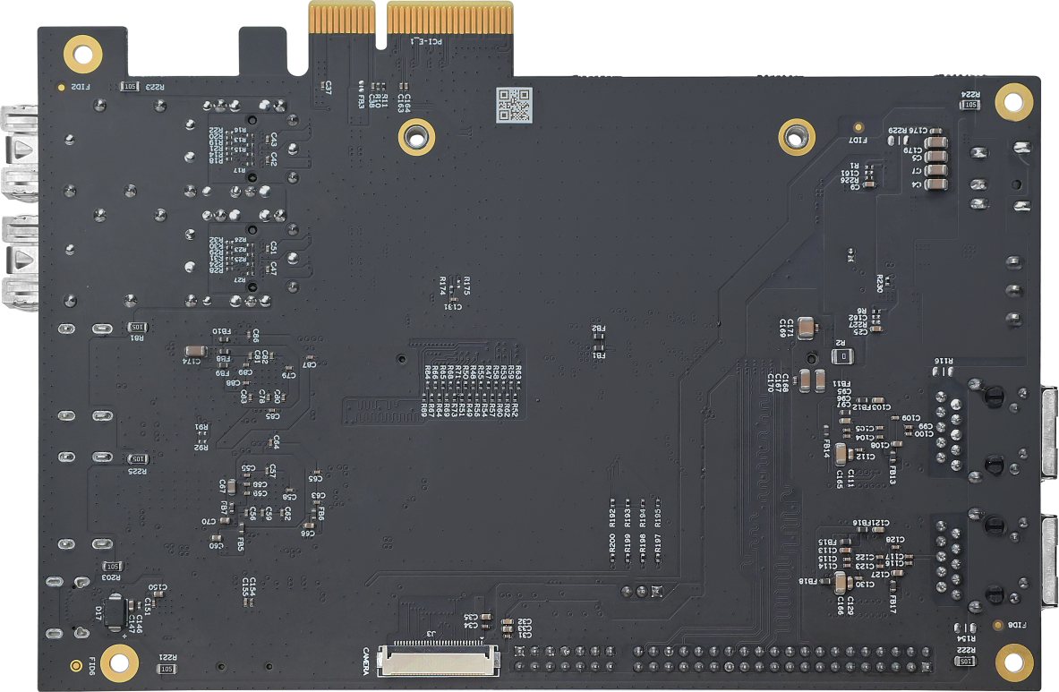
The MYD-J7A100T Development Board Base Board
- 1 x Power jack
- 3 x Buttons
- 1 x Dip switch (for Boot selection and Power On/OFF)
- 1 x Micro SD card slot
- 1 x JTAG interface
- 2 x SFP+ interfaces
- 1 x PCIe 2.0 interface
- 2 x 10/100/1000 Mbps Ethernet interfaces
- 1 x USB-to-UART interface (Type C)
- HDMI input and output
- 1 x DVP digital camera interface
Supports MYIR’s MY-CAM011B Camera Module
- 1 x 2.54mm pitch 40-pin male expansion header
Supports MYIR’s MY-WIREDCOM RPI Module to extend RS232/RS485
Only logged in customers who have purchased this product may leave a review.
Shipping Policy
To minimize or avoid tariffs, we ship from the country where the product is made, such as China, Italy, or Taiwan. We sell worldwide in USD.
Fast Delivery! We ship via FedEx, UPS, DHL, and USPS because they're fast, reliable, and easy to track. We process orders within 24 hours, and delivery may take 4-7 working days, depending on your location. We'll email you the tracking number once your order is shipped. We sell in USD.
Shipping Costs: For some industrial products, such as heavy wheels and CNC machines, we calculate shipping costs by weight rather than quantity. To reduce shipping costs for orders with multiple items, please email us at sales@ozrobotics.com before placing your order. We show shipping rates on the product page under the SHIPPING tab. To view the shipping cost for your country, click 'Add to Cart' on the product page.
Return Policy
5 Hours: Mistakes happen when ordering, so you have 5 hours to request a refund for any reason, including if you don’t want to pay the tariff. However, Stripe will not refund you their processing fee if you cancel your order.
All Sales Are Final: After 5 hours, we cannot cancel your order or issue a refund because order cancellations incur multiple transaction processing fees from Stripe and PayPal, additional shipping fees, and reverse tariff payments, which are costly and time-consuming. For technical issues, we will be happy to assist you in resolving problems and provide a replacement if you can prove that the product has a manufacturing defect.
Exchange Policy: We want you to be happy with your new purchase. However, once you have used the product, we cannot issue a refund. However, we will offer an exchange for a product with irreversible manufacturing defects or technical issues. If you purchased the wrong product, then you, as the customer, will be responsible for the re-shipping fees and tariffs. If the product you purchased is defective, email us at support@ozrobotics.com with photos or a video of the faulty parts so we can evaluate the issue before arranging a replacement.
Privacy Policy
Oz Robotics does not collect personal data from customers or visitors; it collects only the data shown on the user profile screen for registered users.
Terms and Conditions
If you were not at home or at your shipping address during the parcel delivery: It is not our or the supplier's fault; if the shipping/delivery company could not deliver your parcel because you, the customer, were not at home or at your delivery address on the delivery date/time, and as a result, the carrier returned your parcel to the manufacturer from where it was shipped. Please note that we do not accept excuses; you will therefore have to pay the re-shipping fee and the tariff for any re-shipment request. In such a case, we will not issue a refund. Please always check your spam folder to ensure you receive emails from Oz Robotics and shipping companies.
Product Warranty: Our warranty covers only product-related problems caused by manufacturing defects. It does not cover problems resulting from faulty repair attempts, customer accidents, or misuse.
Please check your SPAM folder! To provide you with delivery information, we may add your email address to the shipping website so you are notified of delivery until your parcel reaches your shipping address. Please always check your spam folder to ensure our emails from ozrobotics.com and email notifications from DHL, UPS, FedEx, USPS, or other couriers don't land there. Please let us know if you don’t want us to enter your email address on the shipping company website for event notifications.


Reviews
There are no reviews yet.